

 surface | © Scienta Omicron")
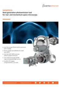
NanoESCA
Next Generation Photoemission Tool for Real- and Momentum Microscopy
PES XPS PEEM EF-PEEM Momentum Microscopy Spin Momentum Microscopy μARPES ARPES Spin-ARPES HAXPES
- Live View energy-filtered real & momentum space imaging
- Precise sample spot definition for small area ARPES
- One-shot 180° ARPES overview without sample movement
- LHe cooled microscope sample stage and dedicated light-sources
- Excellent 2D imaging energy resolution (< 25 meV)
The NanoESCA is an energy-filtering photoemission microscope that can easily switch between the imaging of the momentum space and the real space of photoemission electrons. It’s wide range of measurement modes makes it predestined for momentum microscopy, ARPES of very localised features, and imaging spectroscopy (e.g. with X-ray lab-source or synchrotron).
Photoemission has a history as one of the leading techniques in material and surface science. In the last decade, 2D k-space imaging or "Momentum Microscopy" has become one of the latest and most promising developments in this field. It allows insight into the electron band-structure of novel material systems, unveiling useful effects that can have a strong impact in future information technology. In combination with real-space imaging it is the ideal tool to make new materials applicable to next-generation devices.
Band structure is the key to understanding the working principals of nearly all solid-state devices (transistors, microprocessors, LEDs, solar cells, etc.). New material classes including graphene, topological insulators, and transition metal dichalcogenides (TMDs) are examined for their use in future electronic devices. TMDs, especially, are chemically versatile and thus predestined to tune their electronic structure for various applications. Momentum Microcopy provides a fast band structure mapping, which becomes essential for device engineering in the future.
Momentum Microscopy describes the combination of a photoemission electron microscope (PEEM) with an imaging band-pass energy filter. For kinetic electron energies up to 40 eV the microscope collects all photoelectrons emitted into the complete solid angle above the sample surface. For a discrete energy (selected by the band-pass filter) it forms an image of the photoelectron distribution as a function of the lateral momentum (kx, ky). For example, it is possible to see a full Brillouin zone for certain energies, (e.g. the Fermi surface) in one shot. In live-view mode, it is possible to navigate through the band structure, zoom into details or adjust apertures. By scanning a range of energy filtered momentum maps, one directly gets a 3D data cube (lateral electron momentum vs. electron binding energy) which represents the accessible electronic band structure of the material under investigation.
More Information
How the NanoESCA Works

The extended PEEM lens is designed to easily switch between real-space imaging and momentum-space imaging by switching the projection lens settings. At the same time, the electron trajectories in both modes are equal up to the first image plane. This implies that one can use the two different apertures integrated into the PEEM column. The first one at the back focal plane of the objective lens (contrast aperture) restricts the angular acceptance of the microscope. In real-space imaging this reduces the spherical aberration and thus enhances the resolution of the PEEM. For momentum space imaging it is typically fully open. The second aperture is an iris-aperture. As shown in Figure, it can be used to define a small emitting area on the sample (< 6 μm), from which photoelectrons are measured in momentum mode.

Micro-ARPES as Key-Application
 | © Scienta Omicron")
Besides the imaging energy-filter, the lens extension of the PEEM, which allows one to image the momentum distribution, is the key feature of the Momentum Microscope. This extended PEEM lens is designed to easily change between real-space imaging and momentum-space imaging by switching the projection lens settings. At the same time, the electron trajectories in both modes are equal up to the first image plane. This implies the usage of the two different apertures integrated into the PEEM column. The first one at the back focal plane of the objective lens (contrast aperture) restricts the angular acceptance of the microscope. In real-space imaging, the spherical aberration is reduced and thus enhances the resolution of the PEEM. For momentum space imaging, it is typically fully open. The second aperture is an iris aperture to define a small emitting area on the sample (< 6 µm) from which photoelectrons are measured in momentum mode. The work-flow of micro-ARPES includes finding special features on the sample surface, isolating them by closing the iris aperture around them, and then switching to momentum space mode to complete band structure imaging from a well-defined spot on the sample. This technique does not depend on the beam spot of a light source like conventional ARPES or imaging XPS, which uses a scanning beam spot. To search for features on the sample in real-space mode, the field of view can be zoomed from 800 μm in diameter to 6 μm.
Imaging Spectroscopy in Real-Space
, and secondary electron image of the same sample. | © Scienta Omicron")
Over the last decades standard XPS instruments (ESCA+) have matured towards routine sample analysis and instrument development is dominated mainly by software integration and ease-of-use.
Approaches towards new instrumentation beyond routine XPS sample analysis have been rare and imaging XPS with lateral resolution below 1 µm stayed long out of reach.
The unique approach of a high resolution entrance lens and the revolutionary energy analyser concept (IDEA = imaging double hemispherical energy analyser) allowed NanoESCA to breach this barrier. In contrast to standard secondary electron microscopy (SEM) or x-ray beam induced secondary imaging (SXI) high lateral resolution PEEM imaging with excellent energy resolution allows detailed pre-analysis of the sample far beyond pure sample navigation.
As a result much deeper understanding of the local sample structure, chemistry and electronic structure becomes possible with NanoESCA - an instrument truly designed for imaging.
Scienta Omicron‘s service contracts and worldwide service network provides ready support for our customers in all major markets.
 Measurements at CEA-LETI (Grenoble) | © Scienta Omicron")
Specifications
< 25 meV
0 - 200 eV (up to 10 keV optional)
< 0.02 Å-1
± 2.5 Å-1
± 90° (full solid angle)
< 40 nm
6 ... 800 μm
< 1E-10 mBar
Up to 1E13 ph/s/mm²
< 300 μm
< 2 meV (He I)
Available
x, y, z, azimuthal
< 3 μm
< 40 K .. 600 K
For full specifications and more information about product options, please do not hesitate to contact your local sales representative.
Results
Bi12Rh3Cu2I5: A 3D Weak Topological Insulator with Monolayer Spacers and Independent Transport Channels
Topological insulators (TIs) are semiconductors with protected electronic surface states that allow dissipation-free transport. TIs are envisioned as ideal materials for spintronics and quantum computing. In Bi14Rh3I9, the first weak...
Momentum microscopy of Pb-intercalated graphene on SiC
Intercalation is an established technique for tailoring the electronic structure of epitaxial graphene. Moreover, it enables the synthesis of otherwise unstable two-dimensional (2D) layers of elements with unique physical properties...
Work Function Engineering of Thin α-RuCl3 by Argon Sputtering
α-RuCl3 is a candidate material for the realization of a Kitaev spin liquid with envisioned applications for quantum computing. It is a van-der-Waals material with in-plane honeycomb lattice equivalent to the CrX3 (X= Cl, Br, I) type...
Hydrostatic Strain Enhancement in Laterally Confined SiGe Nanostripes
Strain engineering in SiGe nanostructures is fundamental for the design of optoelectronic devices at the nanoscale. Here we explore a new strategy, where SiGe structures are laterally confined by the Si substrate, to obtain high tensile...
Reference Systems


Downloads
NanoESCA: Next-Generation Photoemission Tool
The Scienta Omicron NanoESCA is a cutting edge instrument with a “Live View” energy-filtered real- & momentum space imaging, offering precise sample spot definition for small area ARPES. The other key features include 1) one-shot 180 degree ARPES overview without sample movement; 2) LHe cooled microscope sample stage and dedicated light-sources; and 3) Excellent 2D imaging energy-resolution.
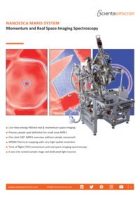
NanoESCA MARIS: Momentum and Real Space Imaging Spectroscopy
Photoemission has established itself as one of the leading techniques in material and surface science. In the last decade, 2D k-space imaging or “Momentum Microscopy” has become one of the latest and most promising developments in this field. It allows insight into the electronic band-structure of novel material systems, unveiling useful effects that can have a strong impact in future information technology. In combination with its real-space imaging capability, NanoESCA MARIS is the ideal tool for investigating the physical properties of materials at the nanoscale, thus enabling the development of next-generation nanodevices.
Highlights from the new NanoESCA MARIS system
In light of FOCUS GmbH’s recent announcement of joining the Lab14 group, we want to assure our mutual customers that the collaborative relationship between Scienta Omicron GmbH and FOCUS GmbH remains unchanged. We are committed to continuing our close partnership, and no changes are anticipated to our relationship as a result of FOCUS GmbH’s restructuring in ownership


