Characterization of Buried Interfaces Using Ga Kα Hard X-Ray Photoelectron Spectroscopy (HAXPES)
Result of the Month
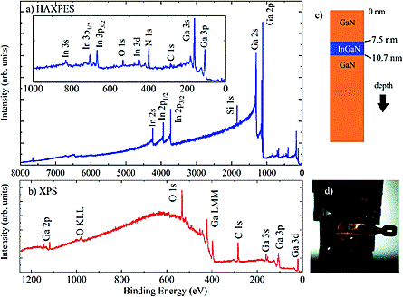
(a) HAXPES (with the low BE region shown in the inset) and (b) Al Kα XPS survey spectra for an InGaN/GaN heterostructure (In0.19Ga0.81N, 3.2 nm thick), as shown in the schematic in (c). (d) Photograph of samples on sample plate on the manipulator.
HAXPES measurements using the 9.25 keV laboratory source, on a set of InxGa1−xN/GaN heterostructures (a quantum well (QW) typically 3 nm thick, with varying In content, on top of 2.5 μm GaN, with a 7.5 nm GaN capping layer) on (0001) sapphire substrates, prepared by metal–organic chemical vapor deposition and characterised using high-resolution transmission electron microscopy and electron energy loss spectroscopy. Figure shows normal emission HAXPES (a) and Al Kα XPS survey spectra (b) for a typical QW structure. As illustrated in (c), containing 19% In (In0.19Ga0.81N) with a 3.2 nm thick QW. XPS measurements were taken at normal emission, and HAXPES using grazing incidence with a photoemission angle of 4° in transmission mode (d). For Al Kα XPS, there is an unfortunate overlap of the N 1s and Ga LMM signals, which is removed at different photon energies. No peaks associated with In are observed using XPS, which is dominated by surface contamination containing carbon and oxygen, whereas In 3s, p, d are observed with HAXPES, along with the deeper core levels In 2s and 2p.

2D angle-resolved data for an InGaN/GaN heterostructure (In fraction of 19%) and a gold reference sample, measured using the AR56 detection mode on the EW4000 analyser. (a) Ga 2p, (b) N 1s, (c) In 2p3/2, and (d) Au 3d5/2 from the reference sample. Increasing photoemission angle indicates increasing surface sensitivity. The intensity colour bar (arb. units) is shown on the right-hand side.
Angle-resolved measurements were performed on two of the heterostructures with In stoichiometries of x = 0.15 and x = 0.19 (QW widths of 2.9 and 3.2 nm respectively). Measurements were carried out using the AR56 mode of the EW4000 analyser, where the usable angular range (to neglect any slit edge effects) is approximately 40°. The sample was tilted so that the angle between the analyser entrance plane and the surface normal was 40°, meaning that photoemission angles in the range 20–60° were captured in a single shot. Minimal depth-resolved information is gained in the range 0–20°; grazing incidence measurements measured at a photoemission angle of 4° provide an additional measurement at the maximum sampling depth.

Zr 3d spectra of an untreated piece of Zr metal, measured using (a) HAXPES (9.25 keV) and (b) XPS (1.486 keV), O 1s spectra measured with (c) HAXPES and (d) XPS, (e) Zr 2p3/2 spectra measured using HAXPES, and (f) valence band spectra measured using HAXPES (black points and line) and XPS (red points and line).
High resolution spectra of Zr 3d, Zr 2p, O 1s and the valence band regions of the untreated Zr sample. The surface sensitive XPS spectrum of Zr 3d shows one spin–orbit split chemical species, with Zr 3d5/2 associated with ZrO2. HAXPES, however, shows two species: a second doublet is present at ca. 4.4 eV lower binding energy (blue), associated with metallic Zr. Similarly, the Zr 2p3/2 peak is comprised of two chemical species (the doublet pair is not shown as the spin–orbit splitting of Zr 2p is relatively large). The BEs of the metallic and oxide species have a similar chemical shift of 4.3 eV, in both Zr core levels. The O 1s spectra show a greater proportion of lattice oxygen (at a lower binding energy, green peak) when measured with HAXPES, because there is lower sensitivity to oxygen-containing contamination (such as hydroxides and oxidised carbon species) at the surface. Finally, the valence band spectra show that HAXPES, sampling the metallic Zr below the oxide passivation layer, measures the Zr 4d core level at a low binding energy.